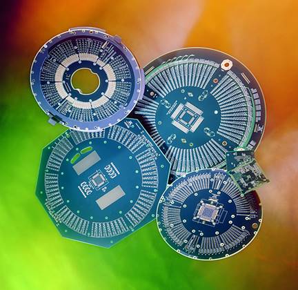
Blair Gordon Associate Inc.

PCB DESIGN

  • High-performance characterization boards
  • Load Boards / DUT Cards / ATE Boards
  • Blank Probe Cards -- Generic and Custom
  • Bench, Evaluation and Demonstration Boards
  • Commercial boards

Capabilities

  • High-Speed Digital design
  • Mix signal design
  • RF design
  • Controlled Impedance transmission line
  • Minimum Crosstalk
  • Multiple impedance transmission lines to minimize the effect of load capacitance
  • Minimum skew between same signal busses
  • Special routing techniques for high-speed transmission lines
Blair Gordon Associate Inc.

Software

  • Cadence Design tool (allegro, PCBrouter)
  • PCAD Design tool
  • Pads Design tool
  • Expedition Router
  • Cam

Available Tester Templates

  • Agilent
  • Credence
  • LTX
  • Teradyne
  • Avnet
  • Schlumberger
  • Checksum
  • Nextest
  • Advantest

DFM Capability Matrix

Blair Gordon Associate Inc.
A picture of the inside of an electronics device.

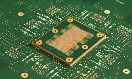
PCB FABRICATIONS & PCB ASSEMBLY

Outsource Fabrication to the top high-end approved worldwide PCB/PWB Fabricators

Capabilities

  • Panel / board sizes to 24”x30” (~22”x28” finished)
  • Mixed dielectrics
  • Layers 50 +
  • Max board thickness .300”
  • Drill sizes down to 0.004”
  • BGA pitch to 0.4mm
  • Drill aspect ratios w/o multi-lam 31:1
  • Min finished lines/spaces .002”/.002”
  • Impedance tolerance +/- 5%
  • Blind and buried vias (Silver fill or non-conductive epoxy fill)
  • Materials
  • Lamination Cycles up to 5 sequential
  • Metal Finishes Ni/Au (hard), Ni/Au (soft), Brt Ni, ENIG
  • Bow & twist available to 0.002in/in
  • Filled Via Flatness +/-.0005
  • Filled Via Aspect Ratio 31:1
Blair Gordon Associate Inc.

Add On Services

  • DRC in Genesis
  • Net list check
  • Extensive quality control system
  • 1000 Volt electrical test
  • 7 Day standard cycle time – non-filled probe PCBs
  • DFM training for PCB design
  • Stack-Up services
Blair Gordon Associate Inc.

Contact for More Information